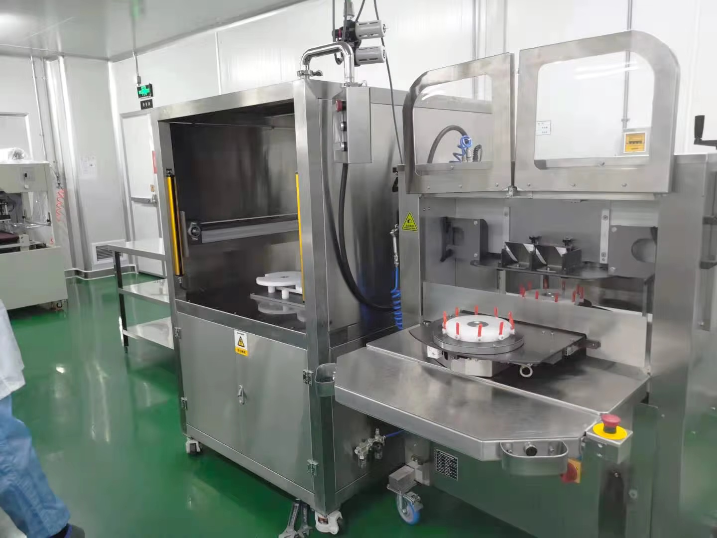
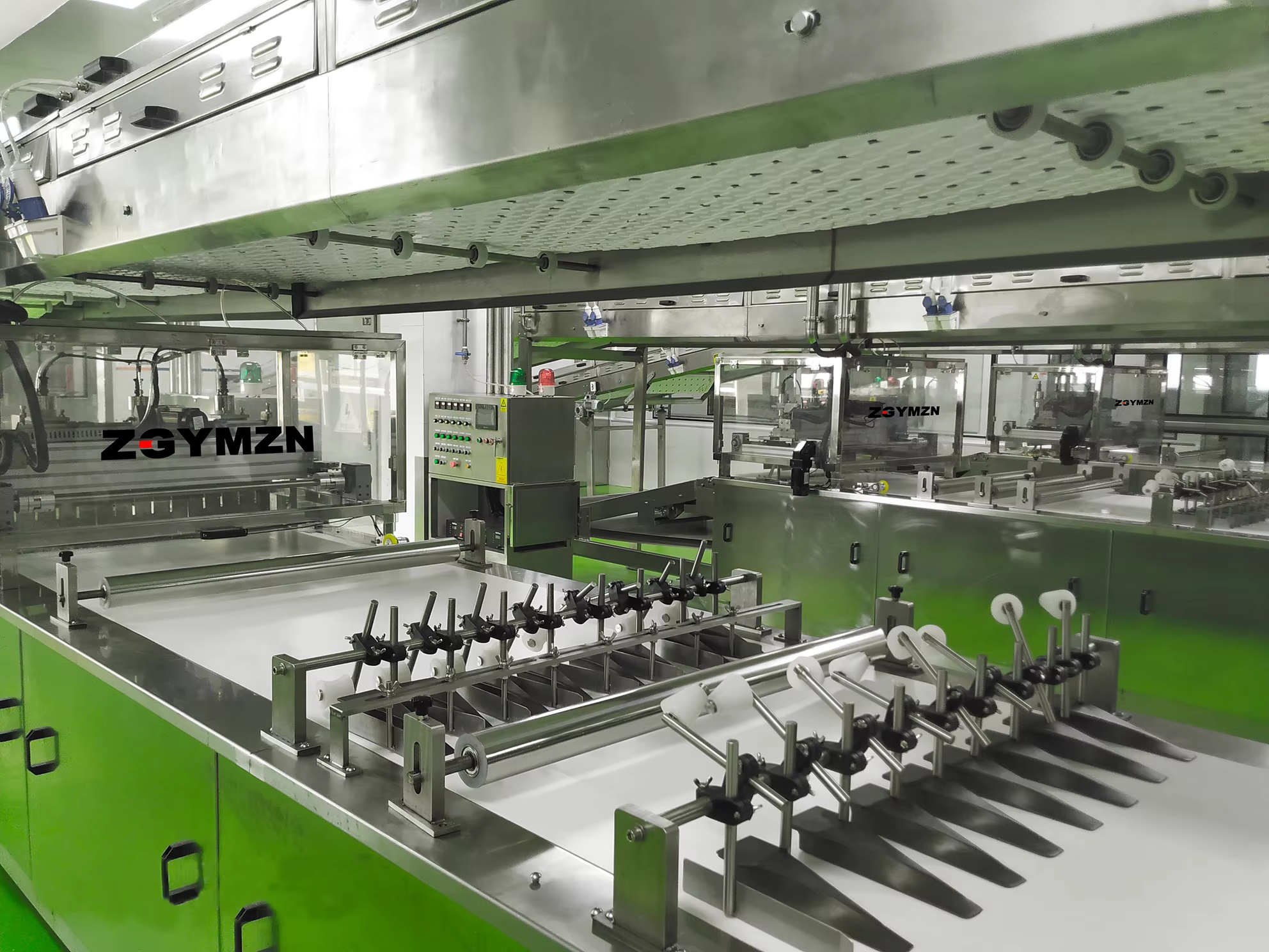
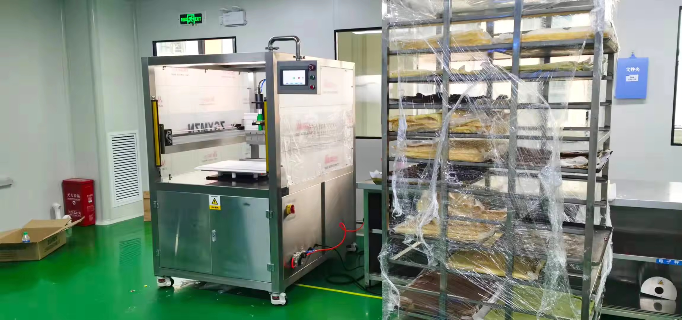
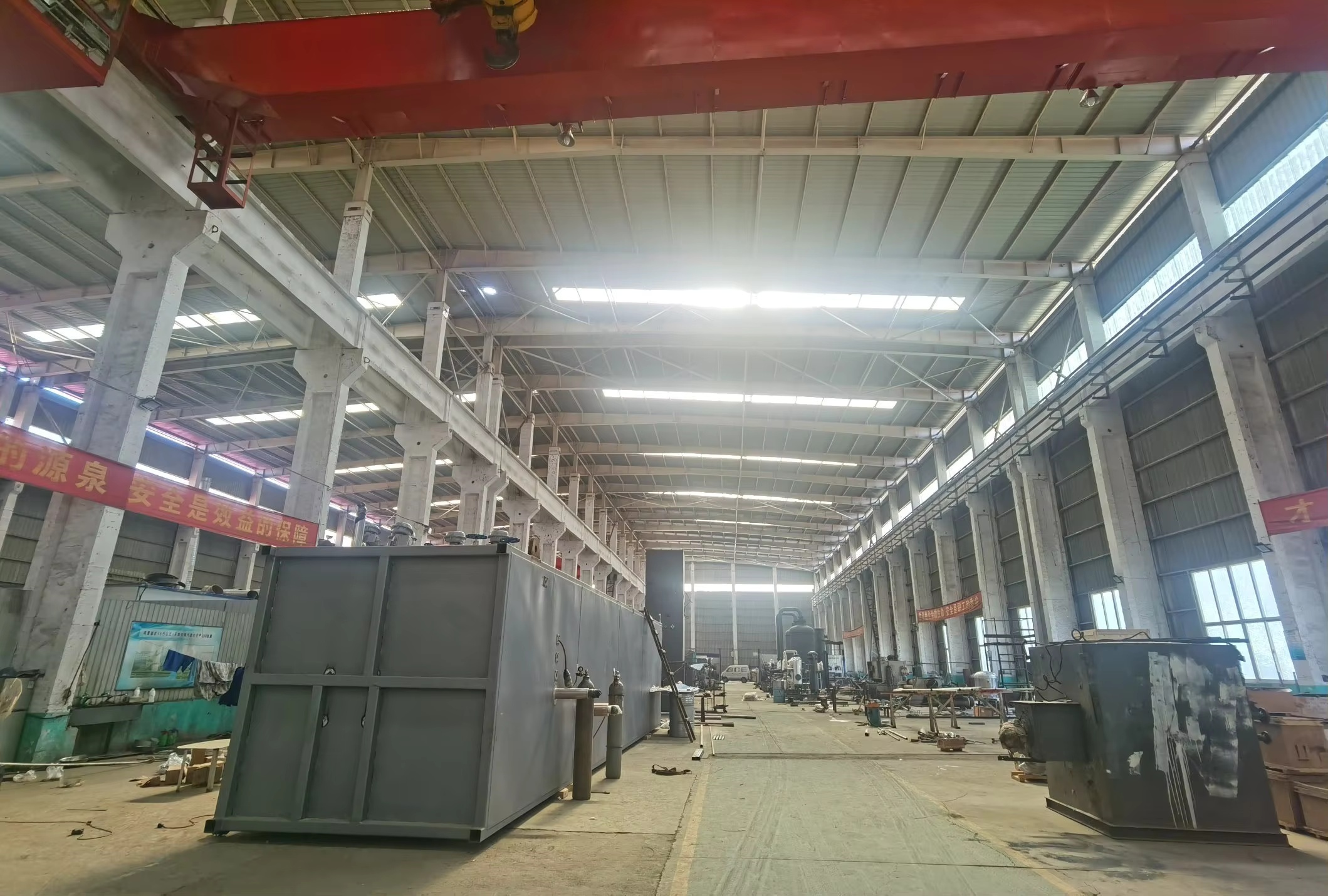
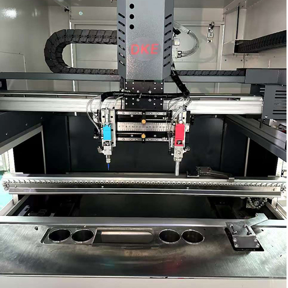
Looking to contact semiconductor manufacturer teams for wet process equipment? Meraif supports Southeast Asia buyers with solutions for silicon wafers, IC wafers, advanced packaging, IC substrates, and SMT—backed by patented nozzle technology, vacuum negative pressure spray cleaning, and supercritical fluid expertise for high-precision semiconductor cleaning.
-
Room 1504, Unit 3, Building 1, Tianjian Yuewanfu, Nanshan Subdistrict, Nanshan District, Shenzhen, Guangdong, China
Quality Wet Process Equipment for Semiconductor
Meraif provides complete wet process equipment solutions for semiconductor manufacturing, from silicon wafers and IC wafers to advanced packaging, IC substrates, and SMT. Our patented nozzle technology, vacuum negative pressure spray cleaning, and SCF capabilities are designed to improve cleaning performance, protect wafers, and support cleaner, more sustainable production.


Key Features & Advantages
Patented Nozzle Technology
Vacuum Negative Pressure Spray Cleaning
Water-Free, Wastewater-Free Process Direction
SCF Capability for Advanced Processing
Product Specifications
| Parameter | Specification |
|---|---|
| Company | Meraif |
| Established | 20+ years |
| Headquarters | China |
| Manufacturing Network | 3 factories and multiple domestic and international offices |
| Solution Scope | Comprehensive wet process equipment solutions for silicon wafers, IC wafers, advanced packaging, IC substrates, and SMT processes |
| Core Cleaning Technology | Patented nozzle technology engineered for semiconductor cleaning applications |
| Cleaning Performance Focus | Higher cleaning efficiency and improved cleaning results versus conventional nozzles, with wafer-safe particle and contamination removal |
| Spray Cleaning Method | Vacuum negative pressure spray cleaning inside a vacuum environment |
| Environmental Process Design | Distillation recovery with a water-free and wastewater-free process approach |
| Advanced Process Capability | Supercritical Fluid (SCF) technology integration |
| Market Coverage | Mainland China, Taiwan, Japan, South Korea, and Southeast Asia |
Manufacturing & Quality Control
Headquartered in Shenzhen, with 3 factories and multiple offices at home and abroad, Meraif supports customers across Mainland China, Taiwan, Japan, South Korea, and Southeast Asia. This footprint helps customers source from a partner with both manufacturing depth and regional responsiveness.
Quality on this page is demonstrated through engineering proof: proprietary nozzle design, semiconductor-focused cleaning know-how, vacuum-based spray process design, and environmentally conscious recovery methods. Rather than relying on generic claims, the page centers on measurable process capability and operational scale.


Applications / Solutions
Silicon Wafer Processing
IC Wafer Applications
Advanced Packaging
SMT Processes
Frequently Asked Questions

Meraif is a comprehensive solution provider for full-series wet-process equipment used in semiconductor and electronics manufacturing. Based on the supplied company profile, its strength lies in supporting silicon wafers, IC wafers, advanced packaging, IC substrates, and SMT processes with specialized cleaning and wet-process technologies.
For Meraif, the strongest verified positioning is its role as a wet-process equipment solution provider serving multiple semiconductor manufacturing stages. On this page, that translates into engineering depth, process coverage, and factory-backed execution rather than unsupported claims about manufacturing models not stated in the supplied company information.
The supplementary company text provided for this page does not confirm China Semiconductor Industry Association membership. To keep the page accurate and trustworthy, this claim should be added only when current active membership can be verified.
Because Meraif already serves customers across Mainland China, Taiwan, Japan, South Korea, and Southeast Asia. That regional reach helps buyers understand the company’s commercial coverage, delivery capability, and ability to support cross-border semiconductor and electronics manufacturing projects.
Because buyers look for verifiable ecosystem signals. CSIA presents itself as a national industry association covering design, manufacturing, materials, equipment, research, education, and applications, so current membership can reinforce credibility when it is real, active, and linked to proof. (CSIA)
It tells buyers that the supplier can support both proprietary semiconductor/device programs and OEM manufacturing requirements. In practical sourcing terms, that suggests fewer handoff points, closer engineering-to-quality coordination, and better control over specification changes across the production cycle. This is an inference based on how the IDM model is structured.
